Current Research:
Terahertz technology is a fast-growing field with wide range of applications in material spectroscopy and sensing, imaging, radio astronomy,
high-data-rate short range communications and others. Located between millimeter-wave and infrared, the Terahertz band is scientifically
rich but as of yet a not fully explored part of the electromagnetic spectrum.Our current research is focused on a number of projects including:
- THz photoconductive antennas
- THz Fourier transform spectroscopy
-
Novel THz devices/antennas based on 2D materials and meta-surfaces
-
mmWave radar imaging
Past Research:
-
Improving the conversion efficiency of THz photoconductive
sources using nano-structures:
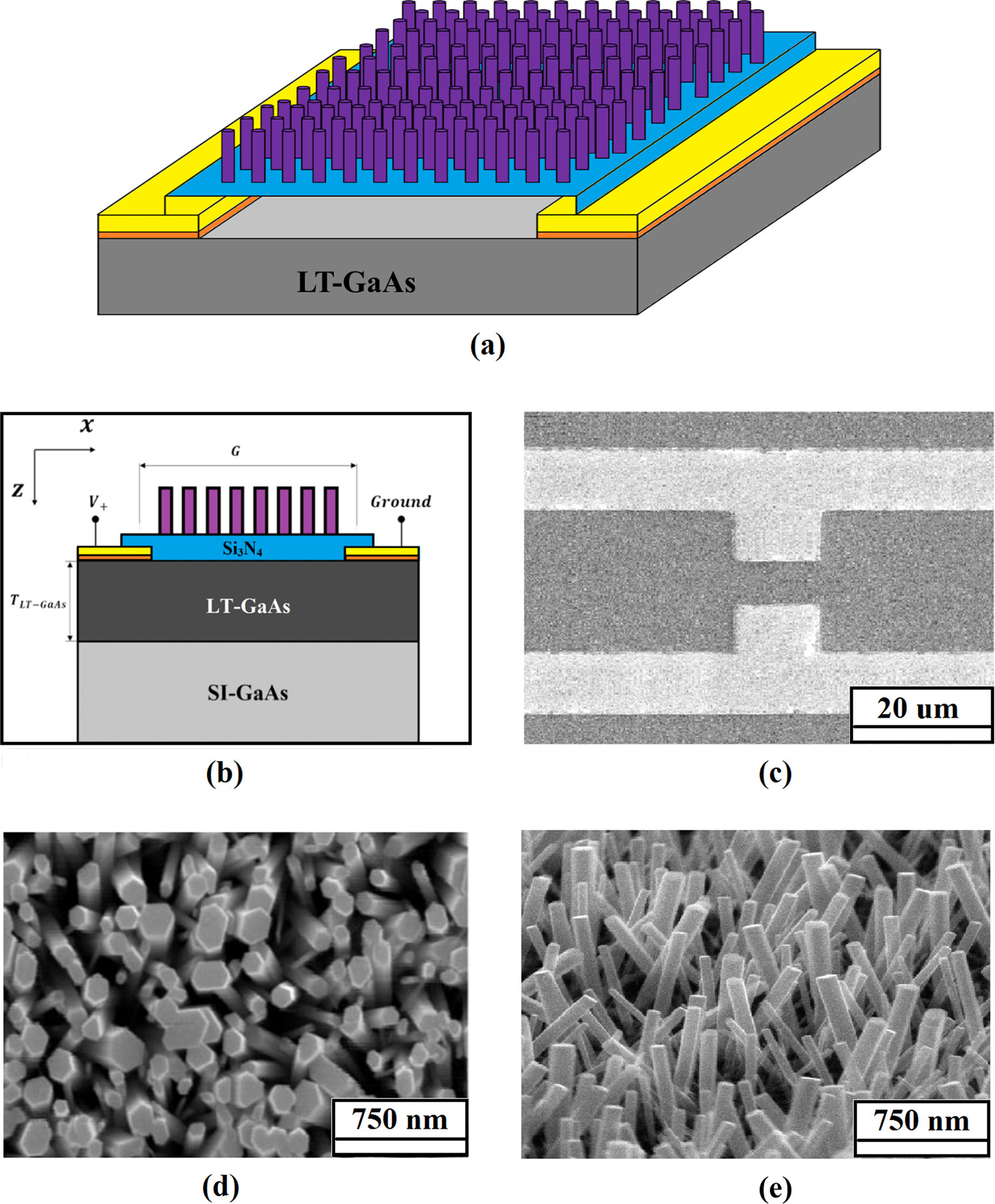 An
efficient terahertz (THz) photoconductive antenna (PCA), as a major
constituent for the generation or detection of THz waves, plays an
essential role in bridging microwave-to-photonic gaps. We propose an
impressive approach comprising the use of arrayed zinc oxide nanorods
(ZnO NRs) as an optical nanoantenna over an anti-reflective layer
(silicon nitride) in the antenna gap to boost the photocurrent and
consequently the THz signal. The numerical approach applied in
investigating the optical behavior of the structure, demonstrates a
significant field enhancement within the LT-GaAs layer due to the
optical antenna performing simultaneously as a concentrator and an
antireflector which behaves as a graded-refractive index layer. ZnO NRs
have been fabricated on the PCA gap using the hydrothermal method as a
simple, low cost and production compatible fabrication method compared
to other complex methods used for the optical nanoantennas. Compared to
the conventional PCA with a traditional antireflection coating, the
measured THz power by time domain spectroscopy (TDS) is increased more
than 4 times on average over the 0.1-1.2 THz range. An
efficient terahertz (THz) photoconductive antenna (PCA), as a major
constituent for the generation or detection of THz waves, plays an
essential role in bridging microwave-to-photonic gaps. We propose an
impressive approach comprising the use of arrayed zinc oxide nanorods
(ZnO NRs) as an optical nanoantenna over an anti-reflective layer
(silicon nitride) in the antenna gap to boost the photocurrent and
consequently the THz signal. The numerical approach applied in
investigating the optical behavior of the structure, demonstrates a
significant field enhancement within the LT-GaAs layer due to the
optical antenna performing simultaneously as a concentrator and an
antireflector which behaves as a graded-refractive index layer. ZnO NRs
have been fabricated on the PCA gap using the hydrothermal method as a
simple, low cost and production compatible fabrication method compared
to other complex methods used for the optical nanoantennas. Compared to
the conventional PCA with a traditional antireflection coating, the
measured THz power by time domain spectroscopy (TDS) is increased more
than 4 times on average over the 0.1-1.2 THz range.
 Beside
the above low cost technique, we have developed metallic and dieectric
nona-strauctured patterns to improve conversion efficiency of PCAs.
These contribution resulted in
publications of [J26, J27, J28, J31, C36, C37, C38, C41, C42, C43, C44]. Beside
the above low cost technique, we have developed metallic and dieectric
nona-strauctured patterns to improve conversion efficiency of PCAs.
These contribution resulted in
publications of [J26, J27, J28, J31, C36, C37, C38, C41, C42, C43, C44].
-
Developing THz Devices/Antennas based on graphene:
Recent
emergence of metasurfaces has enabled the development of ultra-thin flat
optical components through different wavefront shaping techniques at
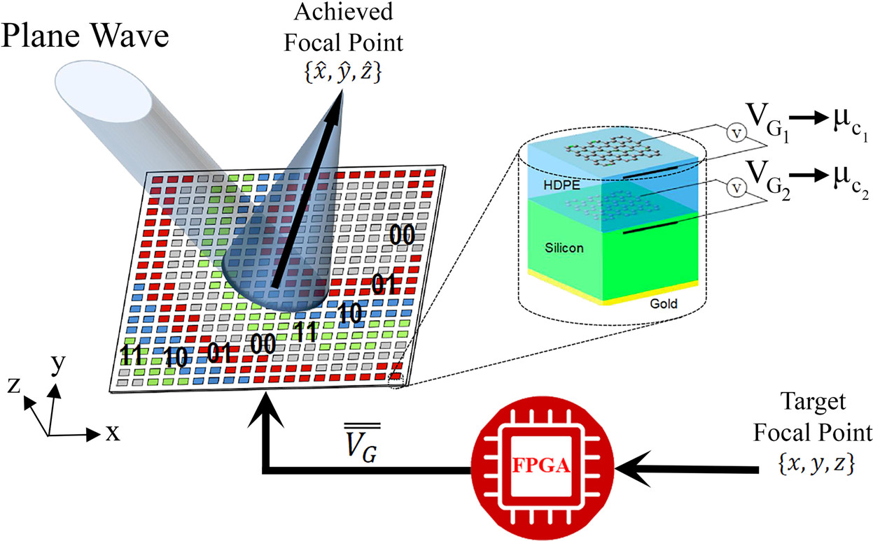 various
wavelengths. However, due to the nonadaptive nature of conventional
metasurfaces, the focal point of the resulting optics needs to be fixed
at the design stage, thus severely limiting its reconfigurability and
applicability. In this work, we aim to overcome such constraint by
presenting a flat reflective component that can be reprogrammed to focus
terahertz waves at a desired point in the near-field region. To this
end, we first propose a graphene-based unit cell with phase
reconfigurability, and then employ the coding metasurface approach to
draw the phase profile required to set the focus on the target point.
Our results show that the proposed component can operate close to the
diffraction limit with high focusing range and low focusing error. We
also demonstrate that, through appropriate automation, the
reprogrammability of the metamirror could be leveraged to develop
compact terahertz scanning and imaging systems, as well as novel
reconfigurable components for terahertz wireless communications. various
wavelengths. However, due to the nonadaptive nature of conventional
metasurfaces, the focal point of the resulting optics needs to be fixed
at the design stage, thus severely limiting its reconfigurability and
applicability. In this work, we aim to overcome such constraint by
presenting a flat reflective component that can be reprogrammed to focus
terahertz waves at a desired point in the near-field region. To this
end, we first propose a graphene-based unit cell with phase
reconfigurability, and then employ the coding metasurface approach to
draw the phase profile required to set the focus on the target point.
Our results show that the proposed component can operate close to the
diffraction limit with high focusing range and low focusing error. We
also demonstrate that, through appropriate automation, the
reprogrammability of the metamirror could be leveraged to develop
compact terahertz scanning and imaging systems, as well as novel
reconfigurable components for terahertz wireless communications.
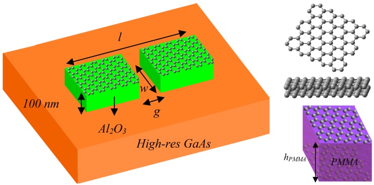 In other works, we have developed antennas based on graphene to make use
of its tunablities in antenna parameters.
These contribution resulted in publications of [J18, J29, J32, C25, C26,
C32, C45, C46].
Developing mid-infrared energy harvesting based on electron
field emission rectification:
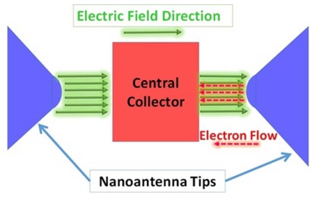 Unlike
the solar energy, infrared radiation from black bodies around us is
always available. In this work, a novel energy harvesting device is
proposed for absorption of the infrared radiation from hot objects
around us at temperatures beyond 300 K, in the vicinity of 10 μm Unlike
the solar energy, infrared radiation from black bodies around us is
always available. In this work, a novel energy harvesting device is
proposed for absorption of the infrared radiation from hot objects
around us at temperatures beyond 300 K, in the vicinity of 10 μm
wavelength, or from the Earth itself. Electron field emission from sharp
edges in vacuum, based on Fowler-Nordheim (FN) theory, is proposed as a
means of rectification. A large number of nanoantennas can be placed in an
array to achieve high electric field, required for FN electron emission.
The issue of wave
spatial coherence is investigated, and it is shown that the
device can operate with small affection.
Using the proposed device, the MIM/MIIM diode, which is usually used for
rectification and has a very low efficiency, is avoided and therefore
efficiency is
highly improved. A planar spiral series nanoantenna array (SSNA) is
designed, as an example, to demonstrate the concept. Bowtie and cross
bowtie antenna
geometries are considered and their performances are compared.
This contribution resulted in publications of [J24,
J30, C40].
-
Study of THz generation based on
laser-induced plasma:
A comprehensive theoretical study is presented on the polarization state
of THz wave radiation from a two-colour laser-induced
plasma and its dependency on  plasma,
optical pulse polarizations and phase difference. We extend the
so-called photocurrent model to calculate three-dimensional distribution
of photocurrent from which the polarization state of the THz radiation
is calculated. It is shown that the calculation results from the
photocurrent model, is in agreement with the previously reported
experiments. Moreover, we show the possibility of creating any desired
polarization state (i.e. elliptical, circular or linear) for the THz
radiation through such generation mechanism by adjusting proper
parameters. This contribution resulted in publications of [J22, C31,
CP2]. plasma,
optical pulse polarizations and phase difference. We extend the
so-called photocurrent model to calculate three-dimensional distribution
of photocurrent from which the polarization state of the THz radiation
is calculated. It is shown that the calculation results from the
photocurrent model, is in agreement with the previously reported
experiments. Moreover, we show the possibility of creating any desired
polarization state (i.e. elliptical, circular or linear) for the THz
radiation through such generation mechanism by adjusting proper
parameters. This contribution resulted in publications of [J22, C31,
CP2].
-
Developing bias-free continuous
wave terahertz photomixer emitters with dis-similar Schottky barriers:
We are introducing a new class of
bias free CW terahertz photomixer
emitter array. Each emitter consists of an asymmetric
metal-semiconductormetal
(MSM) that is made of two side by side dis-similar Schottky contacts,
on a thin layer of low temperature grown (LTG) GaAs, with barrier
heights of difference (ΔΦB) and a finite lateral spacing (s).
Simulations show that when an appropriately designed structure is
irradiated by two coherent optical
beams of different center wavelengths, whose frequency difference (Δf)
falls in a desired THz band, the built-in field between the two
dis-similar
potential barriers can accelerate the photogenerated carriers that are
modulated
by Δω, making each pitch in the array to act as a CW THz emitter,
effectively.
We also show the permissible values of s and
ΔΦB pairs, for
which the strengths of the built-in electric field maxima fall below
that of
the critical of 50 V/μm- i.e., the breakdown limit for the LTG-GaAs
layer.
Moreover, we combined the bias free concept with plasmonic grating
electrodes to enhance the conversion efficiency. This contribution resulted in publications of [J19, J20,
J21, J23, J25, C28, C34, C35, C39].
-
Developing terahertz time-domain spectroscopic ellipsometry (THz-TDSE) system:
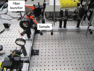
We developed a new instrumentation and calibration procedure for terahertz time-domain spectroscopic ellipsometry (THz-TDSE) that is a newly established characterization technique. The experimental setup is capable of providing arbitrary angle of incidence in the range of 15°-85° in the reflection geometry, and with no need for realignment. The setup is also configurable easily into transmission geometry. For this setup, we successfully used hollow core photonic band gap fiber with no pre-chirping in order to deliver a femtosecond laser into a THz photoconductive antenna detector, which is the first demonstration of this kind. The proposed calibration scheme can compensate for the non-ideality of the polarization response of the THz photoconductive antenna detector as well as that of wire grid polarizers used in the setup. In the calibration scheme, the ellipsometric parameters are obtained through a regression algorithm which we have adapted from the conventional regression calibration method developed for rotating element optical ellipsometers, and used here for the first time for THz-TDSE. As a proof-of-principle demonstration, experimental results were obtained for a high resistivity silicon substrate as well as an opaque Si substrate with a high phosphorus concentration. We also demonstrated the capacity to measure a few micron thick grown thermal oxide on top of Si. Each sample was characterized by THz-TDSE in reflection geometry with different angle of incidence. This contribution resulted in publications of [J9, J13,
J17, C23], and there is a patent on this system [P3].
- Developing high performance antenna
systems in (sub)millimeter wave and THz range:
 In the emerging multi-Gbps and extreme
bandwidth wireless systems, the performance of the antennas has a crucial
impact on the overall performance of the system. Radiation efficiency of an
antenna is one of the main parameters that defines the performance, and is
limited by the power loss in the
 antenna. By increasing the frequency toward
sub-millimeter-wave and THz, the metallic loss becomes dominant.
Therefore, radiation efficiency is degraded in conventional metallic antennas
at mmW/THz frequencies. To overcome such
deficiency, we have studied dielectric antennas as a promising substitution
specially when used in an array arrangement [C5, C12, C15]. The very short wavelengths in the
mmW/THz band has motivated huge interest in exploring
on-chip antenna structures rather than off-chip antenna solutions. On-chip
antenna simplifies the packaging and eliminates pad and bonding parasitics from the high frequency nodes of the circuit
i.e. receiver input and transmitter output, and improves the system
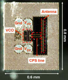
performance. In a collaborative project, we developed a platform for on-chip
integration of high performance antennas with integrated circuit transmitters
working beyond 100 GHz in SiGe technology. The
first generation of this platform including a chip with a 200-GHz VCO
integrated with an on-chip antenna was designed and fabricated, and
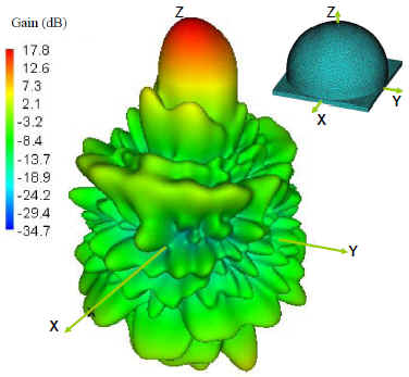
successfully characterized [J7, J8]. Experimentally, a radiated power of 40 μW and antenna gain of 17 dB that was the highest reported gain in Si
technology up to that date at this range of frequency, were measured. antenna. By increasing the frequency toward
sub-millimeter-wave and THz, the metallic loss becomes dominant.
Therefore, radiation efficiency is degraded in conventional metallic antennas
at mmW/THz frequencies. To overcome such
deficiency, we have studied dielectric antennas as a promising substitution
specially when used in an array arrangement [C5, C12, C15]. The very short wavelengths in the
mmW/THz band has motivated huge interest in exploring
on-chip antenna structures rather than off-chip antenna solutions. On-chip
antenna simplifies the packaging and eliminates pad and bonding parasitics from the high frequency nodes of the circuit
i.e. receiver input and transmitter output, and improves the system
performance. In a collaborative project, we developed a platform for on-chip
integration of high performance antennas with integrated circuit transmitters
working beyond 100 GHz in SiGe technology. The
first generation of this platform including a chip with a 200-GHz VCO
integrated with an on-chip antenna was designed and fabricated, and
successfully characterized [J7, J8]. Experimentally, a radiated power of 40 μW and antenna gain of 17 dB that was the highest reported gain in Si
technology up to that date at this range of frequency, were measured.
Developing a
comprehensive approach for modeling and analysis of
integrated terahertz photoconductive devices:
 Modeling and analysis of integrated
terahertz photoconductive sources is a multi-faceted
problem. Conventionally, the analysis of such devices dealt
in detail with one aspect of the problem while making
simplistic assumptions about other aspects. For example,
some researchers focus on the details of the electromagnetic
aspect while using simple models of materials and
photo-induced charge carrier dynamics. Or, conversely they
concentrate on the details of the materials and charge
transport, but apply simple models of the electromagnetic
fields inside the device. Using these conventional
approaches does not provide the level of the accuracy
required for many applications.
 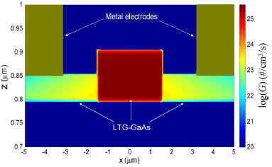 During the course of this project, a
comprehensive method was developed that incorporates all important physical
phenomena that contribute to the operation of photoconductive THz devices.
The aim was to raise the analytical accuracy, and yet keep the complexity at
a reasonable level. The significance of this contribution is that a universal
and geometrically independent approach was developed for the first time for
accurate analysis of terahertz sources [J4]. All major
physical phenomena involved in the operation of such devices are included in
three interconnected solvers, which are combined as a unified analysis tool.
A photonic solver was developed to find the optical intensity across the fast
photo-absorbing region from which the carrier generation rate is determined.
A semiconductor solver was used to study the charge carrier transport inside
the photoconductive region through drift-diffusion model, and to predict the
generated photocurrent with the beat frequency of two continuous-wave (CW)
lasers. An electromagnetic solver was then introduced to rigorously calculate
the coupled terahertz signal into the guiding transmission line or radiating
antenna. This contribution resulted in publications of [J2, J4, J11, J5, C2, C3,
C7, C11, C14]. During the course of this project, a
comprehensive method was developed that incorporates all important physical
phenomena that contribute to the operation of photoconductive THz devices.
The aim was to raise the analytical accuracy, and yet keep the complexity at
a reasonable level. The significance of this contribution is that a universal
and geometrically independent approach was developed for the first time for
accurate analysis of terahertz sources [J4]. All major
physical phenomena involved in the operation of such devices are included in
three interconnected solvers, which are combined as a unified analysis tool.
A photonic solver was developed to find the optical intensity across the fast
photo-absorbing region from which the carrier generation rate is determined.
A semiconductor solver was used to study the charge carrier transport inside
the photoconductive region through drift-diffusion model, and to predict the
generated photocurrent with the beat frequency of two continuous-wave (CW)
lasers. An electromagnetic solver was then introduced to rigorously calculate
the coupled terahertz signal into the guiding transmission line or radiating
antenna. This contribution resulted in publications of [J2, J4, J11, J5, C2, C3,
C7, C11, C14].
- Electromagnetic modeling of the DNA
nano-layers
in THz biochips:
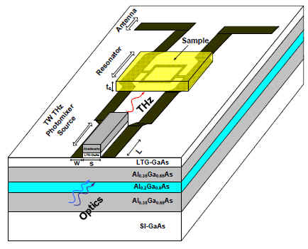 Recent studies on the interaction of THz radiation with bio-molecules
have shown that it is feasible to sense and distinguish bio-molecules from
their unique dielectric properties in the THz range. Based on this principle,
we proposed a continuous-wave (CW) THz biochip using a THz resonator for
label free DNA analysis [J6, J14, C4, C8, C19].
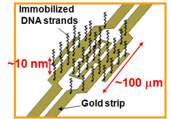 In numerical simulation of THz biochips, modeling
of a self-assembled monolayer immobilized on a metallic surface is a
challenging task. Most of the numerical techniques such as finite element
method (FEM) fail to give accurate results, when the monolayer is modeled as
a thin film dielectric. This failure is due to an extremely large aspect
ratio introduced in the biochip structure, since the thickness of the
monolayer (in the range of nanometers) is much smaller than the
transducer dimensions (in the range of hundred micrometers). To circumvent the aforementioned numerical
problem, we proposed an alternative approach for modeling the mono-layers
[J6, C10]. our approach was based on the equivalent surface impedance
boundary condition. Using the equivalent surface impedance boundary condition
instead of a thin dielectric layer eliminates the mesh generation along the
thickness of the layer, and consequently makes the simulation faster and more
accurate. we applied, for the first time, the concept of surface impedance
for electromagnetic modeling of DNA self-assembled monolayer to evaluate the
performance of resonance-based terahertz biochips in terms of analytic
sensitivity and selectivity [J6]. The proposed model is general and can be
applied to any resonant transducer with metallic surface for receiving thin
film samples. In numerical simulation of THz biochips, modeling
of a self-assembled monolayer immobilized on a metallic surface is a
challenging task. Most of the numerical techniques such as finite element
method (FEM) fail to give accurate results, when the monolayer is modeled as
a thin film dielectric. This failure is due to an extremely large aspect
ratio introduced in the biochip structure, since the thickness of the
monolayer (in the range of nanometers) is much smaller than the
transducer dimensions (in the range of hundred micrometers). To circumvent the aforementioned numerical
problem, we proposed an alternative approach for modeling the mono-layers
[J6, C10]. our approach was based on the equivalent surface impedance
boundary condition. Using the equivalent surface impedance boundary condition
instead of a thin dielectric layer eliminates the mesh generation along the
thickness of the layer, and consequently makes the simulation faster and more
accurate. we applied, for the first time, the concept of surface impedance
for electromagnetic modeling of DNA self-assembled monolayer to evaluate the
performance of resonance-based terahertz biochips in terms of analytic
sensitivity and selectivity [J6]. The proposed model is general and can be
applied to any resonant transducer with metallic surface for receiving thin
film samples.
-
Developing whispering gallery mode
resonance sensor for dielectric sensing:
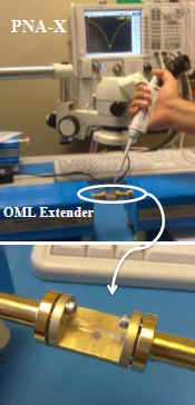 For the first
time, we proposed the application of Whispering Gallery Mode (WGM)
perturbation technique in dielectric analysis of pharmaceutical tablets [J3].
Based on WGM resonance, a low-cost high-sensitivity sensor in THz/mm-wave
frequency range was invented [P2]. We have conducted a comprehe
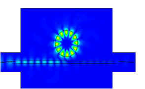 nsive
theoretical and experimental analysis to show that a change in the order of
10-4 in the sample dielectric constant is detected by the proposed
sensor. Various experiments were carried out on drug tablets to demonstrate
the potential multifunctional capabilities of the sensor in moisture sensing,
counterfeit drug detection, and contamination screening. The developed sensor has a great impact on the
quality control and quality assurance in the pharmaceutical industry; and
there is a patent pending on this technology [P2]. Moreover, we have demonstrated simple high
sensitivity sensor devices for liquid sensing in mm-wave range [J1, J10, C9, C13,
C18]. This technique can be used to classify a large number of small-sized
(bio)chemical samples in liquid or solution form based on the differences in
type, concentration or any other property which is related to dielectric
constant and/or dielectric loss of the sample in the mm-wave and THz range. nsive
theoretical and experimental analysis to show that a change in the order of
10-4 in the sample dielectric constant is detected by the proposed
sensor. Various experiments were carried out on drug tablets to demonstrate
the potential multifunctional capabilities of the sensor in moisture sensing,
counterfeit drug detection, and contamination screening. The developed sensor has a great impact on the
quality control and quality assurance in the pharmaceutical industry; and
there is a patent pending on this technology [P2]. Moreover, we have demonstrated simple high
sensitivity sensor devices for liquid sensing in mm-wave range [J1, J10, C9, C13,
C18]. This technique can be used to classify a large number of small-sized
(bio)chemical samples in liquid or solution form based on the differences in
type, concentration or any other property which is related to dielectric
constant and/or dielectric loss of the sample in the mm-wave and THz range.
Last Updated: March 2019
|
|
|